Example of a Microprogrammed Computer
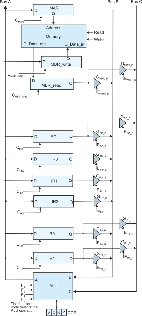
In this example we are going to create a simple 16-bit computer that uses three buses
A, B, and C. Bus C receives its input from the ALU and provides an output to all
registers. Buses A and B provide inputs to the ALU, and receive their inputs from
registers. All registers are connected to bus B, but only some registers are connected
to bus C.
The computer has two general-purpose registers R0 and R1, and three instruction registers
I0, I1 and I2. There is a memory address register, MAR, and two memory buffer registers,
MBR_read and MBR_write, The difference is that MBR_read receives data from memory
during a read cycle, and MBR_write provides data to memory in a write cycle.
A key feature of the ISA (instruction set architecture) of this processor is that
all instructions are three words long: an op-code, an address, and an operand. Both
the address and operand are 16 bits wide and this solves the problem of operand range
(it’s the same as the register width), and addressing range (the full 16-bits are
supported).
The form of instructions supported are:
Register-to-register: MOVE R0,R1, ADD R0,R0,R1
Register-to-memory: MOVE 0x1234,R0 , ADD 0x1234,R0
Memory-to-register: LOAD R0,0x1234, ADD R0,0x1234
Indexed memory: MOVE R0,0x1234(R1) etc
Literal: ADD R0,#0x1234 etc
The classes of instruction are:
- Data movement
- Jump: JMP 0x1234, JMP R0, JMP 0x1234(PC), JMP 0x1234(PC,R0)
- Data processing: Arithmetic, shift, logical, compare
- Conditional branch
The instruction format is:
Bits Function
15 – 13 Predicate
12 – 10 Instruction class
9 – 8 Source register
7 – 6 Destination register
5 – 2 Instruction parameter
1 – 0 Constant 0 to 3
The control signals are:
- Memory: read, write
- Registers: 9 clock, 11 tri-state enables
- ALU: 4 function selects.
The fetch cycle
The fetch phase of each instruction requires the reading of three consecutive words,
even if the instruction does not need all three words. If we assume that the contents
of the PC point to the next instruction to be fetched, the fetch phase can be represented
as:
[MAR] ¬ [PC]
[PC] ¬ [PC] + 1
[MBRread] ¬ [M[MAR]]
[IR0] ¬ [MBRread]
[MAR] ¬ [PC]
[PC] ¬ [PC] + 1
[MBRread] ¬ [M[MAR]]
[IR1] ¬ [MBRread]
[MAR] ¬ [PC]
[PC] ¬ [PC] + 1
[MBRread] ¬ [M[MAR]]
[IR2] ¬ [MBRread]
Having fetched the instruction as three words, the next step is to execute it. Let’s
look at a few operations.
ADD R0,R1 defined as [R0] ¬ [R0] + [R1]
In this case, we only have to copy R0 and R1 to the B and C buses, set the ALU function
code to add, and then clock R0; that is ER0_B, ER0_C, F(add), CR0
Suppose the instruction had been ADD R0,P. In this case, we would have to read address
P from instruction register IR1 and use it to access memory; that is,
[MAR] ¬ [IR1]
[MBRread] ¬ [M[MAR]]
[R0] ¬ [MBRread] + [R0]
The sequence of microoperations corresponding to this are:
EIR1_B, F(pass), CMAR
Read, CMBR_read
ER0_B, EMRread_C, F(add), CR0
Let’s consider a more adventurous ADD R0,(R1,0x1234). In this case we are using address
register indirect with indexing. The index value is in register IR2. The RTL form
of the instruction is [R0] ¬ [R0] + [M[[R1] + [IR2]]. So, we first have to add up
the contents of pointer R1 and instruction register IR2 containing the offset.
EIR2_B, ER1_C, F(add), CIR2 ; This gives us the operand address in IR2
EIR2_B, F(pass), CMAR ;now proceed as before
Read, CMBR_read
ER0_B, EMRread_C, F(add), CR0
Finally, consider a literal ADD R0,0x1234 represented by [R0] ¬ 0x1234. This could
not be easier because it is the same as adding two registers, except that one is
instruction register IR1. That is, is ER0_C, EIR1_B, F(add), CR0
Now for a store literal indexed in memory that uses two constants; that is, STORE
(0x1234,R0),0x5678. The RTL version is [[R0] + 0x1234] ¬ 0x5678. Here we use both
instruction registers IR1 and IR2.
EIR2_B, ER0_C, F(add), CMA2 ; This gives us the operand address of R0 + IR2 in the
memory address register
EIR1_B, F(pass), CMBR_write ; Put the literal in IR1 in the memory buffer register
for writing
Write ;and write to memory
Brand and Jump Operations
This class of instructions all lead to the reloading of the program counter. The
program counter can be loaded from instruction register IR1 (absolute jump), a data
register (register indirect jump), program counter plus IR1 (relative address) or
even program counter plus register (program counter register indirect). Moreover,
we can make loading the program counter dependent on the condition codes to provide
conditional branching.
Let’s consider a conditional program counter relative branch of BEQ target which
is expressed as
IF Z THEN [PC] ¬ [PC] + [IR1]
The sequence of microoperations for this instruction is remarkably simple.
EIR1_B, EPC_C, F(add), IF Z = 1 THEN CPC ; This generates a new address and clocks
the PC if the Z-bit is set.
Extending the Processor
We can extend the processor is two simple ways to increase its flexibility. First,
we are going to give it a return address register to allow simple returns from a
subroutine, and, second, we are going to add a stack pointer.
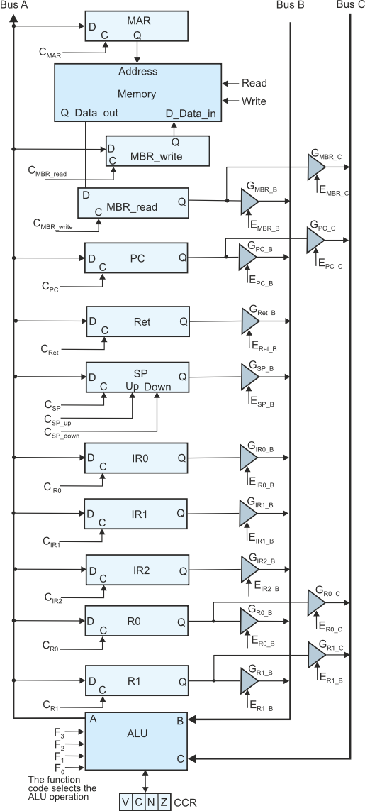
We have created a stack pointer, SP, that can be loaded from the A bus, and its output
deposited on the B bus. The stack pointer is an up/down counter and it provides up-clock
and a down-clock inputs. These allow us to increment it and decrement it, respectively.
The Ret register can be used to store subroutine return addresses. Consider the instruction
pair CALL target and RETURN. The RTL forms of these are:
CALL target: [Ret] ¬ [PC]; [PC] ¬ [PC] + [IR1]; Save PC and add target offset to
the PC to call subroutine
RETURN: [PC] ¬ [Ret]
We can implement these in terms of the following microoperations.
CALL target: EPC_B, F(pass), CRet ;save return address
EIR1_B, EPC_C, F(add), CPC ;jump to new address
RETURN: ERet_B, F(pass), CPC ;restore return address to PC