Boolean Algebra and Circuit Design -
This article presents an extended example of a typical problem you may encounter in a digital design class. For practical reasons, many problems tend to have four variables, because less than four variables presents a rather trivial problem and more than four variables makes it harder to use the traditional Karnaugh map technique to simplify an equation (although you can use Karnaugh maps with up to six variables).
The Problem
Typically, a problem is given in words. In this case, we wish to design a circuit
that receives a 4-
a. Draw a truth table to represent this problem
b. Write down a Boolean equation for F directly from the minterms of the truth table
c. Draw a Karnaugh map to represent this problem from the truth table
d. Derive a simplified expression for F using the Karnaugh map
e. Derive a simplified expression for F using Boolean algebra
f. Draw a logic circuit to implement your solution using AND, OR and NOT gates
g. Draw a logic circuit to implement your solution using NAND gates only
h. Draw a logic circuit to implement your solution using NOR gates only
i. Suppose that inputs representing integers 0, 1, 3, 14, 15 could never occur. Design a simplified expression for F in this case taking advantage of these don’t care conditions.
j. The simplified output from the Karnaugh map is obtained as a sum of products form. Convert this sum of products form into the corresponding product of sums form.
Part a.
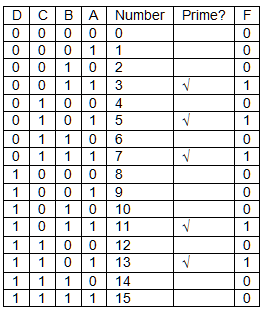
The prime numbers in the range 0 to 15 are 3, 5, 7, 11, 13. We will represents the
4 bits by D,C,B,A (D is the most-
The truth table below gives al 24 = 16 possible combinations of the four variables representing the integers 0 to 15. We have marked primes with a tick and hap put a 1 to output column to indicate that the output is true if the corresponding input is applied. There are five 1s because there are five integers that are prime.
The Truth Table
Part b.
Obtaining a logical expression
Each of the terms in the truth table is called a minterm and contains each of the four variables in either its true or complemented form. For example, D×C×B×A is a minterm, whereas D×B×A is not a minterm because it contains only three of the four variables.
In this case there are five minterms
![]()
The output is true if any of the minterms are true; that is, the output is the Boolean OR of the minterms. Consequently,
![]()
Part c.
Generating a Karnaugh Map
We now draw a Karnaugh map for this system. We will step through the creation of
a Karnaugh map step-
Figure 1 illustrates the structure of a 4-
Note the sequence along the rows and columns: it’s 00, 01, 11, 10 and not 00, 01, 10, 11 as you might expect. Remember that only one variable changes between adjacent rows and columns.
Figure 1 The 4-
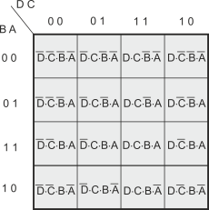
Figure 2 illustrates the situation after we have plotted the minterms from the truth table. I have included the number of each square (i.e., the corresponding line in the truth table) in blue in the upper right hand corner in order to make the placing of the minterms clear. Generally, most students don’t write in minterm numbers in this way (but it can sometimes be a big help).
Figure 2 Plotting the minterms
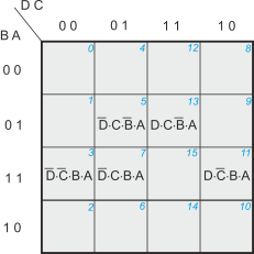
Traditionally, the minterms of a Karnaugh map are represented by a 1. All the other squares contain a 0. However, we do not write down the zeroes because they are ‘understood’. Figure 3 shows the Karnaugh map with 1s representing the lines in the truth table with a 1 in the F column.
Figure 3 The Karnaugh map corresponding to the Truth Table
The key to solving a Karnaugh map problem is to regroup all the 1s. Sometimes this is not always possible and you can’t rearrange the 1s. If that happens, the Boolean equation cannot be simplified further.
The 1s in a Karnaugh map must be grouped into twos, fours or eights (you can have 16 in a group but that would correspond to F = 1; that is, the function is always true). The groups must be a vertical line or a horizontal line, or a square, or a rectangle. Note that the Karnaugh map is topologically a torus (doughnut) so that the upper and lower edges are adjacent as are the left and right edges. This means that a minterm on the bottom row is adjacent to a minterm on the top row vertically above it. All the four corners of a Karnaugh map are adjacent.
Each 1 on the Karnaugh map MUST be in a group, but it may be shared by several groups; that is, the same element (minterm) may be part of several groupings.
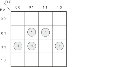
In this case, we can regroup the 1s as figure 4 demonstrates. There are three groups of two 1s; two groups are horizontal and one vertical. Note that one horizontal group (in blue) shares the two edges (because these are actually adjacent). One minterm, is in two groups.
Figure 4 Forming groups of 1s
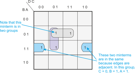
We can now write down a simplified expression for F. We ask what variables are common to each group and then sum the three groups. For example, the blue group contains the common elements B = 1, A = 1, C = 0. Note that D is not in this group because it is 0 in the left hand element and 1 in the right hand element.
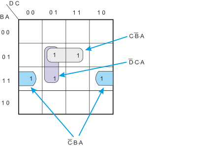
Figure 5 shows the same Karnaugh maps but with the larger groups relabeled.
Figure 5 Labelling the groups of minterms
Part d.
Generating a Simplified Expression for F
Finally, we can write down the simplified equation for F as:
![]()
As you can see, this is a simpler expression than the original sum of five minterms obtained from the truth table.
Part e
Using Boolean Algebra to Simplify and Expression
Now we need to simplify the original expression, the sum of minterms from the truth table, using Boolean algebra. To do this, we use the rules of Boolean algebra until we cannot simplify the expression further. Doing this takes practice and it is rather difficult to tell whether you have a simplified expression or not. You have to practice solving Boolean equations until you become proficient. With a Karnaugh map, the solution is clear because you either can or cannot form bigger groups or fewer groups. Note that neither Karnaugh maps nor Boolean algebra may lead to a unique solution. Sometime it is possible to express a Boolean equation on more than one way.
![]()
We can treat this as conventional algebra and factor the groups; for example,
![]()
Since the sum (logical or) or a variable and its complement is 1, we can rewrite the expression as
![]()
We can perform another re-
![]()
Proceeding as before we get:
![]()
Next we re-
![]()
![]()
![]()
Further simplification is not possible. By the way, suppose we compare this with the simplified function from the Karnaugh map; that is
![]()
Confusingly, these two expressions are not the same but they are logically equivalent. This is because the same Boolean function can sometimes be represented in more than one way (as we pointed out earlier).
Suppose we plot this simplified function on a Karnaugh map. We get the system described by Figure 6. You can see that the 1s on Figure 6 are in exactly the same place as those of Figure 5. The difference is in the way in which the groups are formed. In both cases we have formed the smallest number of large groups. Consequently, both results are correct and equally valid.
Figure 6 The Karnaugh map corresponding to
![]()
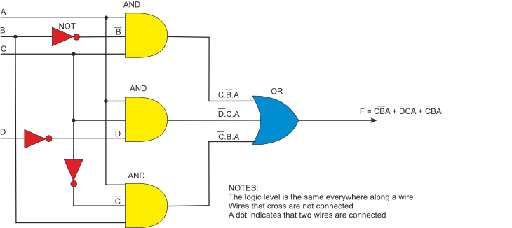
Part f.
Designing a Logic Circuit
To create a circuit using AND, OR and NOT gates. We use NOT gates to perform inversion, AND gates for multiplication and OR gates for addition. As in conventional algebra, the multiplication has a higher priority than addition so that X×Y + P×Q must be done as (X×Y) + (P×Q) and not X(Y + P)Q.
Figure 7 illustrates a circuit using AND, OR and NOT gates.
Figure 7 Implementing the simplified function with AND, OR and NOT gates
Converting and expression in a sum of products form (SoP) is very easy. The SoP form consists of a group of product (AND) terms that are summed (ORed); for example;
![]()
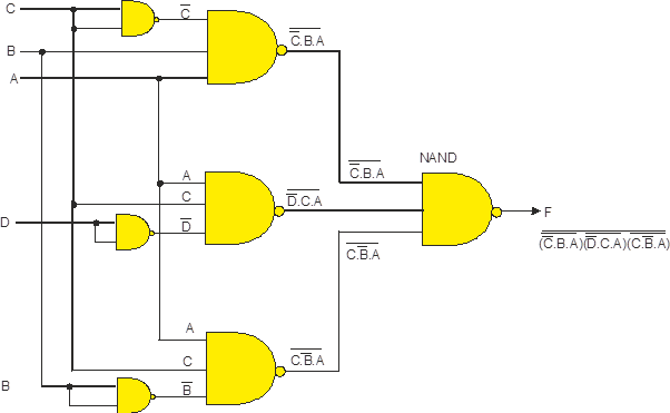
Part g
Constructing the circuit with NAND gates only
It is possible to construct any logic circuit from NAND gates only (or NOR gates only) because de Morgan’s theorem provides a means or translating product terms into sum terms, and vice versa. Consider P = Q×R×S
If we invert this expression twice, we get
![]()
Remember that if we complement an expression twice, its value does not change. However, AND terms and changes to OR terms and individual elements are complemented.
In our example we can write:
![]()
We can now apply deMorgan’s theorem to get:
![]()
Note how we have converted the sum expression into a product expression. Now we are left with only product expressions and inversions.
The transfer function of a 2-
If we make Q = R we get
![]()
Consequently, we can use a NAND gate as a simple inverter.
We can now start constructing the circuit. First note that the entire expression
is inverted and we have three terms ANDed. This means that we must use a 3-
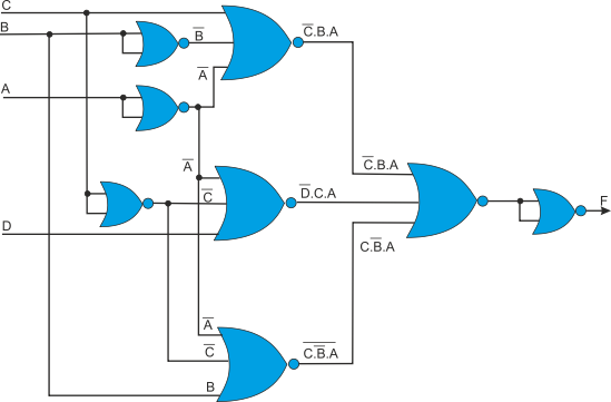
Figure 8 Implementing the simplified function with NAND gates only
Part h
Constructing a Circuit with NOR Gates Only
Designing a circuit with NOR gates only uses the same basic techniques as designing a circuit with NAND gates; that is, the application of deMorgan’s theorem. The only different between NOR gate design and NAND gate design is that the former must eliminate product terms and the latter must eliminate sum terms.
Let’s return to the original expression.
![]()
Note that the output is just a negated NOR expression. We can do the negation with
a 2-
![]()
Finally, we can construct the NOR-
Figure 10 A NOR Gate Only Circuit
Part i
Don’t Care Conditions
Sometimes certain input conditions cannot occur; for example, they may represent physically impossible states or conditions, or choices that are not available. Consequently, if such conditions cannot occur, it does not matter whether we choose those conditions to make the output 0 or 1. However, we can choose the output to be 0 or 1 according to which helps generate the simplest solution.
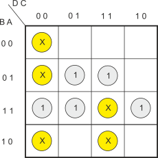
Consider figure 11 where we’ve plotted the don’t core conditions 0,1,2,3,14,15 are xs in yellow circles.
Figure 11 Don’t Care Conditions
If you examine Figure 11 you will find that we can take one of the don’t care conditions (i.e., input represents 15) and create the groups of Figure 12.
Figure 12 Choosing Don’t Care Conditions to Simplify the Karnaugh Map
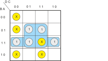
In this case the simplified Karnaugh map gives
F = C.A + B.A
This is a considerably simpler expression than the one we originally obtained and
can be used to build a less expensive logic circuit with fewer gates (in this case
just two 2-
Part j
Converting Sums of Products into Product of Sums Forms
Converting between SoP and PoS forms invariably means converting AND operations into OR operations and vice versa. The only way of doing this is to use deMorgan’s theorem.
Consider the original simplified expression for F
![]()
We can invert this expression twice as the complement of a complement is the original value; that is
![]()
We have applied deMorgan’s law using the inner negation to remove the OR operators. Now let’s apply deMorgan’s law a second time to remove the outer negation.
![]()
We now have the required product of sums form for F. Note that this is not a standard product of sums form because the output is negated. This form would be useful where the output stage of the circuit was a NAND gate.