DRAM
DRAM, dynamic random access memory has provided bulk of high-
DRAM is read/write random access memory and requires a more complex processor interface
than static random access memory. Very simple systems (e.g., controllers and embedded
systems)) may use static memory to avoid the cost and complexity of DRAM controller.
DRAM stores data as a charge on a capacitor which leaks away in several milliseconds.
Consequently, dynamic memory must be continually refreshed to re-
DRAM History
The world’s first DRAM memory device was created by Robert H. Dennard, an IBM Fellow
in 1966 when he and his team were investigating the properties of field-
The first commercial DRAM chip was developed by a new semiconductor company that had been formed two years earlier by Noyce and Moore who left Fairchild Semiconductors. The new company was called Intel and it initially developed a static RAM using bipolar logic and then a static RAM using MOS logic in 1969. In 1970 Intel announced a 1 Kbit (that’s 256 bytes) DRAM memory component called the 1103. This was the world’s first commercial DRAM component and by 1972 it was the best selling memory chip in the world and was rapidly replacing existing magnetic memory systems (ferrite cores).
Another step along DRAM’s path towards domination of the memory market was the introduction
of Mostek’s MK4096 DRAM in 1973. Mostek was founded in 1969 by former employees of
Texas Instruments. The MK4096 was a 4 Kbit chip that introduced address multiplexing.
Static RAMs, both then and now, use a full n-
Over the years, DRAM has evolved. However, DRAM is still essentially the same as it always was; it’s a memory cell that stores a single bit as a charge on a leaky capacitor. Some aspects have changed such as the bit density per chip, the way in which interfacing and refreshing is carried out, and the way in which DRAM is accessed. The access time of DRAM has improved over the years, but the speedup of DRAM over decades is woefully small compared with the way in which processors have advanced.
The term Memory Wall has been coined by Bill Wulf and Sally McKee in 1994 to describe the mismatch between processor performance and memory performance; for example, average memory access times were projected to be 2 cycles in 2000 and 100 cycles in 2010. This represents a factor of 50 in the relative reduction of memory performance. In practice, the situation did not turn out to be quite so bad. Improvements in cache design and performance have helped to hide DRAM’s limitations, and the Memory Wall puts too much emphasis on access time (latency) rather than throughput (bandwidth). Although access time has not increased as much as we would like, the way in which data is moved into and out of DRAMs has permitted a much higher bandwidth. The river doesn’t flow any faster, but at least its wider..
Although the volume of DRAM production has been increasing steadily, the number of DRAM manufacturers has been in decline for the past 20 years. DRAM production is immensely expensive (the cost of fabrication plants) and very competitive. To a great extent, production has moved from West to East and most of the volume manufacturers are now in Asia. In the 1980s major DRAM producers were:
AMD Eurotechni Hitachi Intersil
AMI Fairchild IBM Samsung
AT&T Fuijitsu Infineon Winbond
Elpida Hynix Intel Zilog
By 2009 the major DRAM manufactures were
Elpida PowerChip
Hynix Promos
Micron Samsung
Nanya Winbond
The DRAM Memory Cell
Let’s look at a DRAM memory cell. The classic crossed-
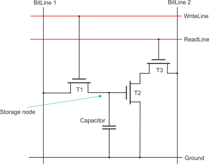
A write operation is performed by asserting the WriteLine and BitLine 1 simultaneously to charge or discharge the capacitor. A charge is transferred to or from the capacitor via transistor T1.
A read operation is performed by sensing the voltage on the capacitor via transistors T2 and T3. The read is carried out by asserting the ReadLine and then sensing the voltage on BitLine2.
Essentially, this three-
The three-
The following figure illustrates the one-
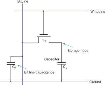
As in the case of the three-
When transistor T1 conducts, the storage capacitor Cs is connected to the bit line. You might think that the voltage on the bit line is the same as that originally stored on the capacitor. However, the bit line has its own capacitance to ground that is distributed along the bit line and its connections. Consequently, the two capacitors CB and CS form a voltage divisor. The voltage that is sensed is proportional to CS/(CS + CB).
Reading the data from a one-
MORE TO FOLLOW