Introduction to Gates and Digital Circuits
These notes cover part of the body of knowledge required by the BCS Certificate Exam. Here, we explain what gates are, how they are used, and how simple digital circuits are constructed.
Boolean algebra is the algebra of logic and can be used to design digital systems. Digital systems are constructed from real components such as memory chips and microprocessors. However, all digital circuits such as memory components can be constructed from primitive devices called gates.
Every digital circuit (apart from peripherals and communication systems) can be constructed from nothing other than a large collection of gates. A system as complex as a computer may require billions of gates.
In this article we a look at simple digital circuits that contain only a handful of gates. Here we discuss only combinatorial circuits. A combinatorial circuit has inputs and one or more outputs. The output is a function only of its inputs. If the output is y and the inputs are x0,x1,x2,…xi, then y = f(x0,x1,x2,…xi) where f is some function (i.e., the behaviour of the circuit).
There are other circuits called sequential circuits whose output is a function of both the inputs and the circuit’s previous state. These circuits exhibit memory because the output depends on what has happened prior to the current inputs. The most obvious example of a sequential circuit is the counter. The next count depends on the previous count. We do not discuss sequential circuits in this article.
Gates
There are three classes of gate: fundamental, derived, and the basic circuit. We look at each of these groups in turn.
Fundamental Gates
There are three basic gates that are derived from the fundamental postulates of Boolean algebra. The AND gate, the OR gate and the NOT gate. All Boolean functions can be implemented with these gates.
Derived Gates
There are two derived gates that can be constructed from an AND gate plus a NOT gate, or an OR gate plus a NOT gate; they are called NAND and NOR gates respectively. The terms NAND and NOR are contractions of Not AND, and Not OR, respectively. The reason that special names were given to these gates is because they both have one very important property. Every digital circuit can be constructed with NAND gates alone; and every digital circuit can be constructed with NOR gates alone.
Another derived gate is the XOR (exclusive OR) gate that can be constructed from two AND gates, two NOT gates, and an OR gate. The XOR gate is of interest because of its mathematical and logical properties and because it is used so frequently in digital circuits.
Basic Circuits
There are an infinite number of circuits that you can construct with gates. Some circuits are so frequently used that they are given names such as the decoder, multiplexer, and adder. Here we will look as some basic circuits (i.e., basic building blocks).
Gate Packages
Gates are available (i.e., manufactured and packaged) in various forms. Consider:
SSI (Small Scale Integration) The very first integrated circuits were called small scale integration and typically included a handful of gates on a single chip; for example, four NAND gates.
MSI (Medium Scale Integration) Medium scale integration chips have sufficient gates to create a basic building block such as an adder or a multiplexer. In general, you would use SSI and MSI circuits to build either a relatively simple digital system (e.g., a burglar alarm or fire alarm) or to connect together more complex systems (e.g., connect a microprocessor to an interface).
LSI and VLSI LSI (large scale integration) and VLSI (very large scale integration) refers to circuits of the complexity of microprocessors. In this article, we are going to look only at SSI circuits.
Fundamental Gates
The AND gate
An AND gate is a circuit with two or more inputs and a single output. It is called an AND gate because the output is true, if and only if, all its inputs are true. That is, if the inputs are A, B, C, the output F is true if A is true and B is true and C is true; that is F = A×B×C.
The simplest AND gate has two inputs; for example F = A AND B = A×B.
By convention a truth table, is often used to illustrate the behaviour of a gate (or circuit). A truth table defines the output for each possible state of the input; for example, a gate with one input has two possible states (0 and 1). A gate with two inputs has four possible states (00, 01,10,11). A gate with three inputs has eight possible states (000, 001, 010, 001, 100, 101, 110, 111). A gate with n inputs has 2n possible states. In general, truth tables are not normally used with systems having more than five inputs because they rapidly grow complex and unwieldy as the number of inputs increases.
Tables 1 and 2 give the truth tables for a 2-
Table 1 The truth table for a 2-
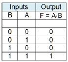
Table 2 The truth table for a 3-
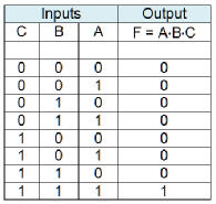
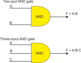
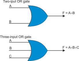
Figure 3 shows the circuit representation of a 2-
Figure 3 Circuit symbols for 2-
One way of looking at the AND gate is to say that it detects an all 1s condition by outputting a 1 when all inputs are 1. Another way of looking at an AND gate is to say that it detects any 0 at an input by outputting a 0 if any input (or more than one input) is 0.
The OR Gate
An OR gate is a circuit with two or more inputs and a single output. It is called an OR gate because the output is true, if any of its inputs are true. That is, if the inputs are A, B, C, the output F is true if A is true or B is true or C is true; that is F = A + B + C. Note that the Boolean OR is not the same as the English language or! Where you say, “Do you want tea or coffee”, you mean one or the other (i.e., the exclusive or). The Boolean OR of three inputs is true for states 001, 010, 100, 110, 011, and 111.
The simplest OR gate has two inputs; for example F = A OR B = A + B.
Table 3 give the truth tables for a 2-
Table 3 The truth table for a 2-
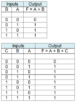
Figure 4 gives the circuit representation of a 2-
Figure 4 Circuit symbols for 2-
One way of looking at the OR gate is to say that it detects an “any 1s condition” by outputting a 1 when one or more of the inputs are 1. Another way of looking at an OR gate is to say that it detects an “all 0s condition” at its inputs by outputting a 0.
The NOT Gate
The NOT gate which is also called an invertor or complementer is the simplest gate: its output is a complement of the input. The truth table for a NOT gate is given below. A NOT gate can have only one input.
Table 4 The truth table for a NOT gate (invertor or complementer)
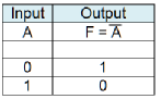
Figure 5 illustrates the NOT gate. Note that the inversion function is indicated by the little circle at the output. In fact, you can put such a circle at the input or output of any gate to indicate inversion.
Figure 5 Circuit symbol for a NOT gate
![]()
Simple Circuits
Before we look at derived gates, we are going to demonstrate some simple circuits. The first circuit in figure 6 uses four gates: three AND gates and OR gate. It has three inputs A, B, C and a single output F.
How do we interpret this circuit? How do we analyse it? What conventions are used when drawing a circuit?
Figure 6 A circuit with four gates
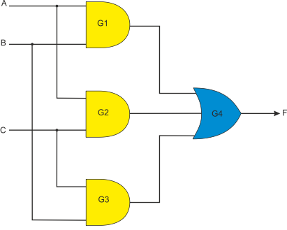
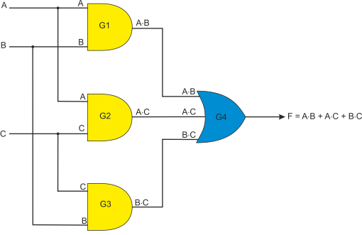
Figure 7 shows the same circuit with some values marked. Let’s begin with the conventions.
The most important aspect of a circuit diagram is its topology; that is, the circuit is all about the connections or paths between circuit elements, and not about how they are laid out or presented. If you were to draw a circuit diagram on a sheet of rubber and then pull, twist and stretch it, it would still have the same topology (and function) even if it looked entirely different.
Figure 7 A labelling signals in the circuit of figure 6
Having pointed this out, there are some practical conventions concerning circuit diagrams. First, signals generally flow from left to right with inputs at the left hand side of the figure; this is done because we write left to right when using the Roman alphabet.
Second, if two circuit paths simply cross, they are not connected. If two paths are connected, a dot is normally placed at their intersection.
Third, the signal level at each point along a path (i.e., wire or printed circuit track) is the same everywhere along that path; a corollary of this is that the same path cannot be driven into two different logical states at the same time.
Figure 7 demonstrates that AND gate G1 receives signals A and B and generates an output A×B. Similarly, gate G2 receives A and C and generates A×C, and gate G3 receives B and C and generates B×C.
OR gate G4 receives inputs A×B, A×C, and B×C, and generates the output F = A×B + A×C + B×C. Incidentally, this expression is in its simplest from and cannot be simplified.
What does this circuit do? Some students may be able to look at the equation and figure out what this represents. However, a more methodical approach is to use a truth table. We’ve got three inputs which means we require a truth table with 8 rows. Consider the table 5.
Table 5 The truth table for the circuit of figure 7
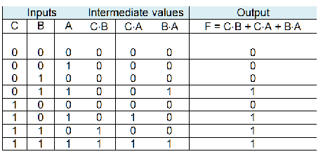
We have tabulated all 8 possible inputs and have provided columns for intermediate values (A×B, A×C, and B×C) together with an output column. Including intermediate values makes it very easy to construct the truth table because we just have to OR them to get the final output F.
So, what does this circuit do? Note that the output is symmetric; there are four 0s and four 1s. The output is 0 of two or three of the inputs are 0, and the output is 1 if two or three of the inputs are 1. In other words, the circuit detects whether the majority of inputs are 0 or 1. It’s a voting circuit, returning a value that corresponds to the larger numbers of 1s or 0s in the input.
Example – Creating a Circuit from an Expression
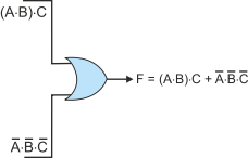
Now let’s consider another example, where we are given a Boolean expression and have to create a circuit. Suppose the expression is F = (A×B)×C + A’×B’×C’ and we have to implement this exactly as in the equation with no rearranging or simplification.
Clearly, the output F is generated from the sum of two product terms; that is, (A×B)×C and A’×B’×C’. We can draw the output of the circuit required to perform this operation (Figure 8).
Figure 8 Creating a circuit from a Boolean expression – step 1
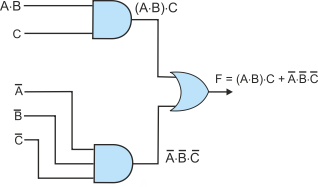
This now leaves us with the two terms (A×B)×C and A’×B’×C’ to generate. These are
both product terms. The first can be generated by a 2-
Figure 9 Creating a circuit from a Boolean expression – step 2
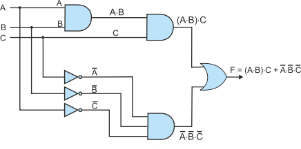
We still have to generate the product term A×B and the negated terms A’, B’, C’. The final circuit diagram, figure 10, demonstrates this last step.
Figure 10 Creating a circuit from a Boolean expression – step 3
Derived Gates
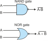
The two most important derives gates are the NAND and NOR gates which are an AND gate followed by an invertor, and an OR gate followed by an invertor, respectively.
The truth tables for 3-
NAND and NOR Gates
Table 6 The truth table for a 3-
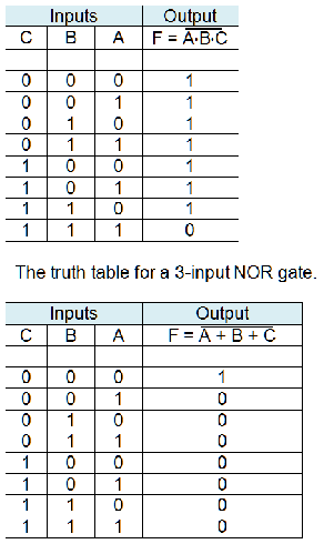
Figure 11 shows the circuit symbols for NAND and NOR gates. The shapes of these symbols are the same as the corresponding AND and OR gates. The only difference lies in the bobble at the output that indicates the inversion operation.
If both inputs of a 2-
Figure 11 Circuit symbols for NAND and NOR gates
Example of a NAND circuit
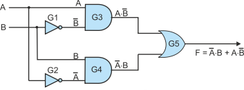
Let’s look at a circuit constructed from NAND gates only, figure 12. This is a classic example because it is found in most textbook and demonstrates how an EOR function (which we will explain later) can be constructed from four NAND gates.
Figure 12 Circuit using four NAND gates
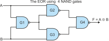
Let’s analyse this circuit. To do this we will introduce intermediate values. Figure 13 includes the addition of intermediate points and an analysis of the signals flowing through the circuit. At each stage (going from left to right) we have presented the output of a gate and then simplified it where possible.
We are left with a final output of F = A×B’ + A×B’. This is the exclusive OR function. It’s called that because it’s rather like the English use of or. The output is true if A alone is true or if B alone is true, but not if both A and B are true. It’s a one or the other circuit. The exclusive or function, XOR, is one of the most important functions in digital systems because it is at the heart of all arithmetic circuits and almost all data encoding and decoding circuits.
Figure 13 Analyzing the circuit using four NAND gates
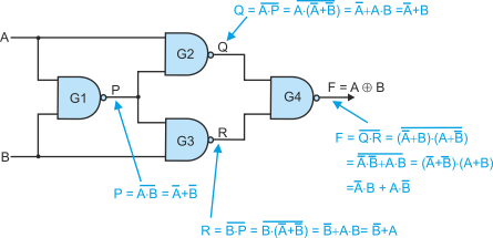
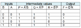
We can also analyse the circuit with a truth table by plotting intermediate values, table 7. This is perhaps easier than the analytic approach in this case. Here the output is F = A×B’ + A’×B which is exactly the same as we derived analytically.
Table 7 Analysing the circuit of figure 13
The Exclusive OR
We have already introduced the exclusive OR (or EOR, XOR – both abbreviations are
commonly used). Figure 14 provides the circuit symbol for an exclusive OR and Table
8 gives its truth table. Most texts describe the exclusive OR as a gate with two
inputs (unlike the AND and OR gates that can have any number of inputs). However,
it is possible to extend the exclusive OR to a circuit with n inputs whose output
is 1 if the number of 1s in the input is odd, and whose output is 0 if the number
of 1s in the input is 0 or even (such a circuit is called an even parity detector).
Here, we discuss only the 2-
Figure 14 The Symbol for the Exclusive OR
![]()
Table 8 Exclusive OR truth table
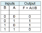
From the truth table we can write F = A×B’ + A’×B. Figure 15 shows how the EOR gate can be constructed using AND, OR and NOT gates.
Figure 15 The EOR Gate constructed from AND, OR and NOT gates
The EOR function performs several functions:
It’s output is 1 if both inputs are different (i.e., 0,1 or 1,0)
It can be used to compare binary values
It calculates the modulo 2 sum of two bits (in modulo 2 arithmetic there is no carry)
Two EOR gates can be used to create a full adder that adds three bits (additional logic is required).
Simple Digital Circuits
The Decoder
A decoder takes an n-
Figure 16 The decoder
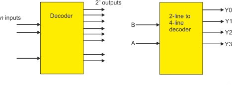
Consider the truth table for the 2-
Table 9 Truth table for the 2-
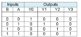
As you can see from table 9, each output is true for one unique value of the input. By inspection, we can write
Y0 = B’×A’
Y1 = B’×A
Y2 = B×A’
Y3 = B×A
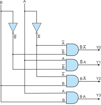
Figure 17 demonstrates how we might implement the decoder. Note that although there are four inversions in the equation, we need only two actual inverters as the figure demonstrates. Once we have inverted A to get A’ we can use it repeatedly in the same circuit.
Figure 17 Implementing the 2-
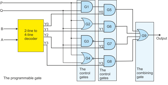
Example of the Use of a Decoder
Here is a simple example of the use of a decoder. It demonstrates how a decoder can
be used to select one of several actions. In this case, we are going to design a
programmable logic element that can perform an AND, OR, NAND and NOR operation depending
on the status of a 2-
You can consider the circuits as using four vertical slices of gates to process the
signals flowing left to right. At the left we have the 2-
The second slice, gates G1 to G4 each take in inputs P,Q to perform a logical function. G1 performs the AND, G2 performs the OR, G3 performs the NAND and G4 performs the NOR. So, at any instant we generate all four functions of P and Q.
The next line of gates G5, G6, G7, G8 are AND gates that perform a gating function (i.e., they pass or block a signal). If the control input (Y0 to Y3) is 0, the output of the corresponding gates is at 0 because X AND 0 = 0. If the control input is 1, then the input from the gate in the previous column is passed because X AND 1 = X.
Finally, all outputs from the control column are passed to G2, the combining gate. Since three of the signals from the control gates must be zero, the output of G9 will be the selected signal from the control gates.
Figure 18 Using a 2-
This circuit has been designed to demonstrate the nature of gates and circuits. The circuit is correct, but we could build a far simpler version by using a truth table (see table 10). We will do that next.
In table 10, inputs B and A perform the programming (logic selection) and inputs P and Q are the logic inputs to be processed.
Table 10 Truth table for a programmable logic element
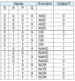
The output is
F = B’×A’×P×Q + B’×A×P’×Q + B’×A×P×Q’ + B’×A×P×Q + B×A’×P’×Q’ + B×A’×P’×Q + B×A’×P×Q’ + B×A×P’×Q’
We can simplify this:
F = B’×A’×P×Q + B’×A×Q’(P’ + P) + B’×A×P×Q + B×A’×P’(Q’ + Q) + B×A’×P×Q’ + B×A×P’×Q’
F = B’×A’×P×Q + B’×A×Q’ + B’×A×P×Q + B×A’×P’ + B×A’×P×Q’ + B×A×P’×Q’
F = (B’×A’ + B’×A)P×Q + A×Q’(B’ + B×P’) + B×A’(P’ + P×Q’)
F = B’×P×Q + A×Q’×B’ + A×Q’×P’ + B×A’×P’ + B×A’×Q’
This circuit could be implemented with four invertors, five 3-
The Multiplexer
A multiplexer is a circuit with several inputs, a control input, and an output. The control input is used to select which input is connected to the output; in other words, the multiplexer is an electronically controlled switch or router. You can think of the multiplexer as the inverse of the decoder we have just described.
The simplest multiplexer is the 2-
IF X == 0 THEN F = A
ELSE F = B
In other words, the multiplexer is a logic circuit that can perform a conditional operation. Ultimately, all computers that implement branch instructions use a circuit that can be considered to be a multiplexer.
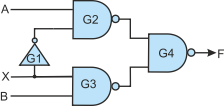
Figure 19 The 2-
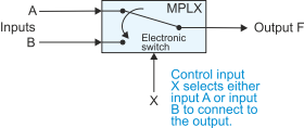
Table 11 gives the truth table for a 2-
Table 11 The truth table for a 2-
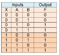
Figure 20 The 2-
This article is available as a PDF file.