Semiconductors
Semiconductors
In this short article I’m going to try and explain how transistors work and how they’re fabricated. This is, of course, an impossible task. All I can do is to provide a faint glimpse into the semiconductor world. Semiconductors are remarkable devices for three reasons. First, they provide the amplification needed to power radios, televisions, computers, and audio circuits. Second, they can be made small; so small, in fact, they you can’t actually see them because they are smaller than visible light itself. Third, they can be connected together in arrays with up to several billion transistors on a single integrated circuit and sold for a few dollars.
Although the details of transistor operation are complex and involve an understanding of quantum mechanics, the basic concepts are quite tractable. Equally, semiconductor manufacturing may involve devices smaller than a wavelength of light, but the fundamental construction mechanism is rather similar to etching or (old film) photography.
Although we are going to discuss silicon transistors, silicon is not the only superconducting material. The first transistors were made of the element germanium.
Silicon and Semiconductors
An insulator like glass, most plastics, and silicon dioxide (sand) does not conduct electricity. Apply a voltage across the ends of an insulator and the electrons do not flow. Apply a voltage across a metal and electrons will flow. Why? Because, it’s all about the relationship between electrons and atoms. An electron orbits the nucleus of an atom in one of several orbits or energy states. The behavior of electrons in solids (molecules and crystals) is more complex than their behavior in isolated atoms because electrons can several energy levels within a given band.
A fundamental property of matter is the energy gap, called a band gap, between adjacent energy bands. It is the size of the band gap that determines the electrical properties of the material.
The outer energy band of an atom is called the valance band. Above this band there is a conduction band that is shared by the atoms of a crystal. An electron in the valence band is bound to its atom. An electron in the conduction band is free to wander.
Insulators have a large band gap and the valence band is full. Electrons cannot move
into the conduction band and move about the crystal lattice. If there are no electrons
in the conduction band, there can be no current because the valence electrons are
bound to individual atoms and can’t go walkabout. The resistance of a good conductor
like silver is 1.59 x 10-
A semiconductor is a material whose resistance falls between that of an instructor and conductor. Although the first semiconductor used to create transistors was gallium, we are going to talk only about silicon.
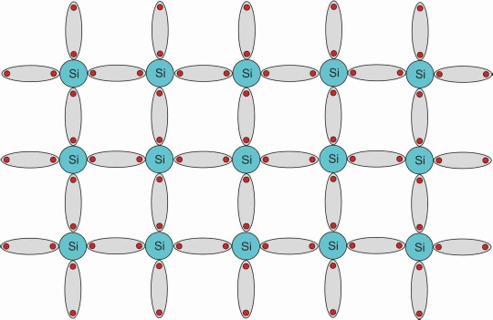
A silicon atom in a silicon crystal is surrounded by four atoms in the valence band and electrons are shared between atoms as Figure 1 demonstrates. This figure is a fiction because the actual molecule is three dimensional, but the principle of sharing four electrons between four adjacent atoms still holds.
Figure 1 The silicon crystal (in two dimensions).
In Figure 1 the valence band electrons are bound to atoms and are not free to move. However, thermal energy can occasionally liberate an electron which then move into the conduction band and become free to move through the crystal. The atom that has lost its electron now has a net positive charge. Such an atom with a missing electron is called a hole (because it’s an empty place that can be filled). A hole is to semiconductors what an overdraft is to a bank account. It is now possible for this atom (the hole) to pick up an electron from a neighboring atom. When this happens, it is as if the hole has moved. Conduction in a semiconductor can be treated as the movement of electrons in one direction or the movement of holes in the other direction.
The number of free electrons generated by thermal energy at room temperature is not
significant. The great invention of semiconductor physics was the addition of tiny
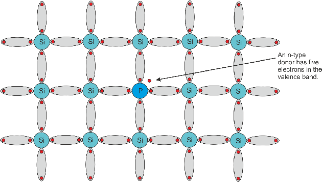
amounts of dopants or impurity atoms to the silicon crystal. There are two types
of dopant; those with 3 electrons in the outer band and those with 5 electrons in
the outer band. Suppose you add a dopant with 5 electrons. Four of these electrons
can join up with the electrons of adjacent silicon atoms in the crystal lattice.
One electron is left over and that electron is free to become a mobile conduction
electron. This impurity is called a donor because it can provide electrons. The resulting
doped silicon is called n-
Figure 2 The n-
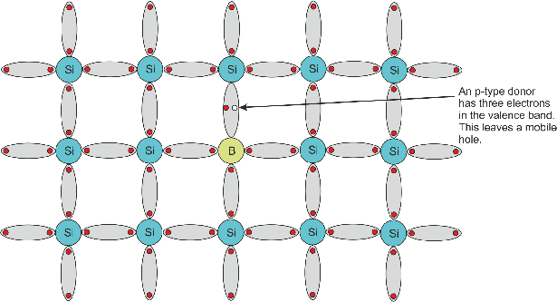
If you perform the same exercise with a dopant with three electrons in the outer
shell, three silicon atoms can join a dopant atom leaving an electron vacancy or
hole. This is called p-
Figure 3 The p-
Let’s repeat this. The addition of very small quantities, one part in a million,
of a dopant to silicon changes the electrical characteristics of the semiconductor
and reduces its resistance by providing electrons or holes as charge carriers. So
far, so pointless. The interesting bit comes when we place an n-
Figure 4 shows three examples of the same pn-
Figure 4 The pn junction
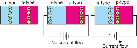
Now consider the effect of applying a voltage across the junction with the positive
terminal connected to the n-
Now consider the right hand configuration with the negative battery terminal wires
to the n-
The pn junction was one of the first semiconductor devices to be manufactured. It
is used to convert AM radio waves into speech, it was used in pre-
In 1947 the bipolar transistor was developed at Bell labs. This device had a double
junction pnp (or npn) made by sandwiching n-
The MOSFET and CMOS
In principle, the MOS transistor is neither conceptually complex, nor difficult to
understand how it is manufactured. However, the precise details of its operation
and manufacture are, to say the least, involved. Figure 5 illustrates the structure
of a MOSFET. The acronym MOSFET means metal-
Figure 5 MOSFET transistor
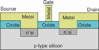
Figure 5 provides a 2D representation of a 3D transistor. We are looking at the transistor
from the side (i.e., it’s a cross section). . There are four terminals (connections):
source, gate, drain, and the substrate (the p-
There are four varieties of MOSFET distinguished by channel type and enhancement/depletion
mode. There are: n-
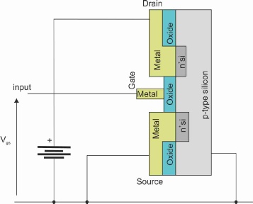
Figure 6 demonstrates the MOSFET of figure 5 in a circuit. The substrate and source
have been connected to ground, 0V. The drain is connected to a positive supply. If
the voltage on the gate is zero, no current will flow through the p-
Let’s state this again. Applying a positive voltage to the gate with respect to the source creates charge carriers under the gate and allows conduction between source and drain. In other words, we have created an electronic switch which is the fundamental element of all logic circuits. If we put two of these transistors in series, current will flow through them only if both gates are driven (AND function). Similarly, if we put two gates in parallel, one across the other, they will conduct if either one will conduct (OR function).
Figure 6 The nMOSFET in a circuit
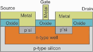
If we reverse silicon types, we can create an inverse transistor that operates in
the same way as the n-
In figure 7 a region or well of n-
Figure 7 The pFET
Putting it all together
If you construct circuits with both pMOS and nMOS transistors, the result is CMOS, complementary metal oxide semiconductor technology. CMOS was patented in 1967 and is the basis of all today’s integrated circuit technology. Essentially, it consists of pairs of pMOS and nMOS transistors in series. If you put these transistors in series, they will never conduct at the same time because the condition necessary to turn one on (the gate voltage) is the condition necessary to turn the other off. Consequently, CMOS technology consumes tiny amounts of power. This is because there is never a path between ground and the positive supply rail through the complementary transistor pair. Figure 8 describes the basis of the CMOS inverter.
The nMOS and pMOS transistors in figure 8 are in series. When the input voltage on the two gates is low (near ground), the lower nMOS transistor is turned off and the upper pMOS transistor is turned on. The output is therefore high, because the pMOS transistor connects the output to the positive rail. On the other hand, when the input is high, the situation is reversed and the nMOS transistor is turned on which forces the output to ground.
Consequently, the output voltage is the inverse of the input voltage and this circuit is an invertor.
Figure 8 The CMOS inverter
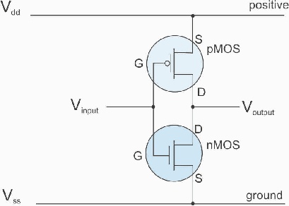
Figure 9 demonstrates how we can construct CMOS NAND and NOR gates. Although we teach students that the NAND gates is created by inverting the output of an AND gate, the inversion happens automatically in CMOS logic which means that a NAND gate is easier to fabricate than an AND gate.
Consider the left hand side of figure 9, the NAND gate. We know that the output of a NAND gate is low if and only if all its inputs are high. Suppose A and B are both 1 (electrically high). The gates of both the lower nFETs are driven positive and the two transistors conduct. They are in series and the output F is pulled down to ground. Note that both inputs to the upper pFETs are high. Because a high input turns off a pFET, both these transistors are effectively disconnected when A = B = 1.
Now, suppose A goes low. The upper nFET will be turned off and the output F no longer
pulled down to ground. Moreover, a low level on A turns on the right-
Figure 9 MOS NAND and NOR gates
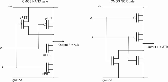
The right hand circuit is a NOR gate and is a mirror image of the NAND gate. The output of a NOR gate is high if both inputs are low. Otherwise, the output is low. If you inspect the NAND circuit you will see that the pFETs are in series and when both inputs A and B are low, the pFETs will be turned on and the output pulled up to a 1. If either input is 1, one or both the series pFETs, will be turned of and one or both of the parallel nFETs will be turned on to drive the output to ground.