The Asynchronous Serial Interface
The vast majority of general-
Figure 1 illustrates the basic serial data link between a computer and a CRT terminal.
A CRT terminal requires a two-
Figure 1 Functional units of a serial data link
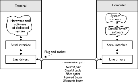
The line drivers in figure 1 translate the voltage levels processed by the ACIA into
a suitable form for sending over the transmission path. The transmission path itself
is normally a twisted pair of conductors which accounts for its very low cost. Some
systems employ more esoteric transmission paths such as fiber optics, or infra-
The two items at the computer end of the data link enclosed in clouds in figure 1
represent the software components of the data link. The lower cloud contains the
software that directly controls the serial interface itself. This software performs
operations such as transmitting a single character, or receiving a character and
checking it for certain types of error. On top of this layer sits the application-
Here we introduce the chip that converts information between the parallel form in which it is processed by the computer and the form in which it is transmitted over the data link. A serial data link operates in one of two modes: asynchronous or synchronous. We describe only the asynchronous data link because synchronous serial data links are best left to texts on networks.
The term character refers to the basic unit of information transmitted over an asynchronous data link. Many data links transmit information in the form of text and the unit of information corresponds to a printed character.
Asynchronous Serial Data Transmission
Until the introduction of USB the most popular serial interface between a computer and its CRT terminal is the asynchronous serial interface. It is so called because the transmitted data and the received data are not synchronized over any extended period and therefore no special means of synchronizing the clocks at the transmitter and receiver is necessary. In fact, the asynchronous serial data link is a very old form of data transmission system and has its origin in the era of the teleprinter.
Serial data transmission systems have been around for a long time and are found in
the telephone (human speech), Morse code, semaphore and even the smoke signals once
used by Native Americans. The fundamental problem encountered by all serial data
transmission systems is how to split the incoming data-
First we examine how the data stream is divided into individual bits and the bits grouped into characters in an asynchronous serial data link. The key to the operation of this type of link is both simple and ingenious. Figure 2 gives the format of data transmitted over such a link.
Figure 2 Format of asynchronous serial data
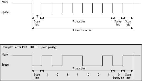
An asynchronous serial data link is character oriented, because information is transmitted
in the form of groups of bits called characters. These characters are invariably
units comprising seven or eight bits of information plus two to four control bits.
Asynchronous data is often transmitted in the form of ASCII-
When the transmitter wishes to send data, it first places the line in a space level (i.e., the complement of a mark) for one element period. This element is called the start bit and has a duration of T seconds. The transmitter then sends the character, one bit at a time, by placing each successive bit on the line for a duration of T seconds, until all bits have been transmitted. After this has been done, a single parity bit is calculated by the transmitter and sent after the data bits. Finally, the transmitter sends a stop bit at a mark level (i.e., the same level as the idle state) for one or two bit periods. Now the transmitter may send another character whenever it wishes. The only purpose of the stop bit is to provide a rest period for the receiver between consecutive characters. This stop bit is a relic of the days of electromechanical receivers, and is not now strictly required for technical reasons. It is there for the purpose of compatibility with older equipment.
As the data word length may be 7 or 8 bits with odd, even, or no parity bit, plus either one or two stop bits, there are a total of 12 different possible formats for serial data transmission. And this is before we consider that there are about seven commonly used values of T, the element duration. Consequently, connecting one serial link with another may be difficult because so many options are available.
At the receiving end of an asynchronous serial data link, the receiver continually monitors the line looking for a start bit. Once the start bit has been detected, the receiver waits until the end of the start bit and then samples the next N bits at their centers, using a clock generated locally by the receiver. As each incoming bit is sampled, it is used to construct a new character. When the received character has been assembled, its parity is calculated and compared with the received parity bit following the character. If they are not equal, a parity error flag is set to indicate a transmission error.
The most obvious disadvantage of asynchronous data transmission is the need for a
start, parity and stop bit for each transmitted character. If 7-
The 6850 Asynchronous Communications Interface Adaptor (ACIA)
One of the first general-
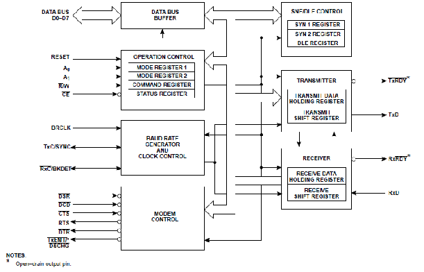
The 6850 ACIA is illustrated in figure 3. I am using this ACIA because it is much easier to understand than newer serial interfaces. Once you understand how the 6850 ACIA operates, you can read the data sheet of any other ACIA.
From the designer's point of view, the 6850's hardware can be subdivided into three sections: the CPU side, the transmitter side and the receiver side. Figure 3 illustrates the functional parts of the 6850 and its internal registers.
Figure 3 The 6850 ACIA

The CPU Side
NOTE: This material is taken from articles I wrote on the 68K microprocessor. Consequently, we describe its interface to the 68K.
The ACIA is a byte-
Unusually, the 6850 does not have a hardware reset input (i.e., a pin that can be
used to clear its internal registers). . Some sections of the ACIA are reset automatically
by an internal power-
The Receiver and Transmitter Sides of the ACIA
One of the great advantages of peripherals like the 6850 ACIA is that they isolate
the CPU from the outside world both physically and logically. The physical isolation
means that the engineer who is connecting a peripheral device to a microprocessor
system does not have to worry about the electrical and timing requirements of the
CPU itself. That is, all the engineer needs to understand about the ACIA is the nature
of its transmitter-
Here, only the essential details of the ACIA's transmitter and receiver sides are
presented, because the way in which they function is described more fully when we
come to the logical organization of the 6850. The peripheral-
Receiver side
Incoming data to the ACIA is handled by three pins, RxD, RxCLK, DCD*. The RxD (receiver
data input) pin receives serial data from the transmission path to which the ACIA
is connected. A receiver clock must be provided at the RxCLK input pin by the systems
designer. This clock may be either one-
The third and last component of the receiver group is an active-
Transmitter side
The transmitter side of the ACIA comprises four pins: TxCLK, TxD, RTS* and CTS*. The transmitter clock input (TxCLK) provides a timing signal from which the ACIA derives the timing of the transmitted signal elements. In most applications of the ACIA, the transmitter and receiver clocks are connected together and a common oscillator used for both transmitter and receiver sides of the ACIA. Serial data is transmitted from the TxD (transmit data) pin of the ACIA to the serial transmission path.
An active-
An active-
Operation of the 6850 ACIA
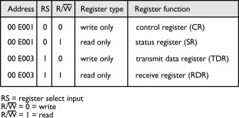
The software model of the 6850 has four user-
Table 1 also gives the address of each register, assuming that the base address of
the ACIA is $00 E001 and that it is connected to the low-
Table 1 Register selection scheme of the 6850
Control Register
Because the ACIA is a versatile device that can be operated in any of several different modes, the control register permits the programmer to define its operational characteristics. This operation can even be performed dynamically, if the need ever arises. However, in almost all applications the ACIA is normally configured once only. Table 2 shows how the eight bits of the control register are grouped into four logical fields.
Bits CR0 and CR1 determine the ratio between the transmitted or received bit rates and the transmitter and receiver clocks, respectively. The clocks operate at 1, 16, or 64 times the data rate. Most applications of the 6850 employ a receiver and transmitter clock at 16 times the data rate with CR1 = 0 and CR0 = 1. For example, if you wish to receive data at 1,200 baud, you must provide a receiver clock input of 16 x 1,200 = 19,200 Hz.
Setting CR1 = CR2 = 1 is a special case and performs a software reset of the ACIA. This operation clears all internal status bits, with the exception of the CTS and DCD bits of the status register. A software reset to the 6850 is invariably carried out during the initialization phase of the host processor's reset procedures.
Table 2 Structure of the ACIA's control register
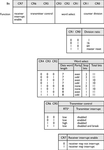
The word select field, bits CR2, CR3, CR4, determines the format of the received or transmitted characters. The eight possible data formats are given in table 2. These bits select also the type of parity (if any) and the number of stop bits. Possibly the most common data format for the transmission of information between a processor and a CRT terminal is: start bit + 7 data bits + even parity + 1 stop bit. The corresponding value of CR4, CR3, CR2 is 0,1,0.
The transmitter control field, CR5 and CR6, selects the state of the active-
IUf the transmitter interrupt is enabled, an interrupt is generated by the transmitter
whenever the transmit data register (TDR) is empty, signifying the need for new data
from the CPU. When the ACIA's clear-
Setting both CR6 and CR5 to a logical one simultaneously creates a special case.
When both these bits are high, a break is transmitted by the transmitter data output
pin. A break is a condition in which the transmitter output is held at the active
level (i.e., space or TTL logical zero) continuously. This condition may be employed
to force an interrupt at a distant receiver, because the asynchronous serial format
precludes the existence of a space level for longer than about ten bit periods. The
term break originates from the old current-
The receiver interrupt enable field consists of one bit, CR7, that enables the generation
of interrupts by the receiver when it is set (CR7 = 1) and disables receiver interrupts
when it is clear (CR7 = 0). The receiver asserts its IRQ* output, assuming CR7 =
1, when the receiver data register full (RDRF) bit of the status register is set,
indicating the presence of a new data character ready for the CPU to read. Two other
circumstances also force a receiver interrupt. An overrun (see later) sets the RDRF
bit and generates an interrupt. Finally, a receiver interrupt can also be generated
by a high-
Status Register
The eight bits of the read-
Table 3 Format of the status register
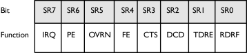
SR0 -
SR1 -
SR2 -
When the DCD* input makes a low-
SR3 -
SR4 -
SR5 -
SR6 -
SR7 -
- Receiver data register full (SR0 set) and receiver interrupt enabled.
- Transmitter data register empty (SR1 set) and transmitter interrupt enabled.
- Data-
carrier- detect status bit (SR2) set and receiver interrupt enabled.
Whenever SR7 is active-
Using the 6850 ACIA
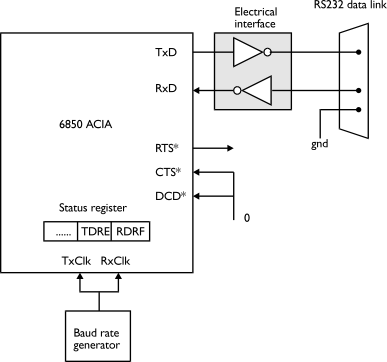
The most daunting thing about many microprocessor interface chips is their sheer complexity. Often this complexity is more imaginary than real, because such peripherals are usually operated in only one of the many different modes that are software selectable. This is particularly true of the 6850 ACIA. Figure 4 shows how the 6850 is operated in a minimal mode. Only its serial data input, RxD, and output, TxD, are connected to an external system. The request to send output, RTS*, output is left unconnected and clear to send, CTS*, and data carrier detect, DCD*, inputs are both strapped to ground at the ACIA.
In a minimal, non-
ACIAC EQU $E0001 Address of control/status registers
ACIAD EQU ACIAC+2 Address of the Tx/Rx data registers
RDRF EQU 0 Receiver data register full
TDRE EQU 1 Transmitter data register empty
INITIALIZE MOVE.B #%00000011,ACIAC Reset the ACIA
MOVE.B #%00011001,ACIAC Set up control word -
RTS interrupts, 8 data bits, even
parity
INPUT BTST #RDRF,ACIAC REPEAT
BEQ INPUT Poll RDRF bit
MOVE.B ACIAD,D0 UNTIL ACIA has data ready
RTS Copy input to D0 and return
OUTPUT BTST #TDRE,ACIAC REPEAT
BEQ OUTPUT Poll TDRE bit
MOVE.B D0,ACIAD UNTIL ACIA is ready for new data
RTS
Figure 4 Using the ACIA in its minimal mode
The INITIALIZE routine is called once before either input or output is carried out
and has the effect of executing a software reset on the ACIA followed by setting
up its control register. The control word %00011001 (see table 2) defines an 8-
The INPUT and OUTPUT routines are both entirely straightforward. Each routine tests the appropriate status bit and then reads data from or writes data to the ACIA's data register.
It is also possible to operate the ACIA in a minimal interrupt-
When a transmitter or receiver interrupt is initiated, it is still necessary to
examine the RDRF and TDRE bits of the status register to determine that the ACIA
did indeed request the interrupt and to distinguish between transmitter and receiver
requests for service. The effect of interrupt-
Figure 5 General-
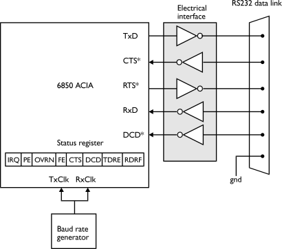
In figure 5 the transmitter side of the ACIA sends an RTS* signal and receives a
CTS* signal from the remote terminal equipment. Now the ACIA is able to say, "I am
going to transmit data to you" by asserting RTS*, and "I know you are ready to receive
my data" by detecting CTS* asserted. In the cut-
Similarly, the receiver side of the ACIA uses the data carrier detect (DCD*) input to signal to the host computer that the receiver circuit is in a position to receive data. If DCD* is negated, the terminal equipment is unable to send data to the ACIA.
The software necessary to receive data when operating the 6850 in its more sophisticated mode is considerably more complex than that of the previous example. It is not possible to provide a full input routine here, as such a routine would include recovery procedures from the errors detected by the 6850 ACIA. These procedures are, of course, dependent on the nature of the system and the protocol used to move data between a transmitter and receiver. However, the following fragment of an input routine gives some idea of how the 6850's status register is used.
ACIAC EQU <ACIA address>
ACIAD EQU ACIA+2
RDRF EQU 0 Receiver_data_register_full
TDRE EQU 1 Transmitter_data_register_empty
DCD EQU 2 Data_carrier_detect
CTS EQU 3 Clear_to_send
FE EQU 4 Framing_error
OVRN EQU 5 Over_run
PE EQU 6 Parity_error
INPUT MOVE.B ACIAC,D0 Get status from ACIA
BTST #RDRF,D0 Test for received character
BNE ERROR_CHECK If char received then test SR
BTST #DCD,D0 Else test for loss of signal
BEQ INPUT Repeat loop while CTS clear
BRA DCD_ERROR Else deal with loss of signal
ERROR_CHECK BTST #FE,D0 Test for framing error
BNE FE_ERROR If framing error, deal with it
BTST #OVRN,D0 Test for overrun
BNE OVRN_ERROR If overrun, deal with it
BTST #PE,D0 Test for parity error
BNE PE_ERROR If parity error deal with it
MOVE.B ACIAD,D0 Load the input into D0
BRA.S EXIT
DCD_ERROR Deal with loss of signal
BRA EXIT
FE_ERROR Deal with framing error
BRA EXIT
OVRN_ERROR Deal with overrun error
BRA EXIT
PE_ERROR Deal with parity error
EXIT RTS
The 68681 DUART
The 6850 ACIA is a first-
- The DUART provides two independent asynchronous serial channels and replaces two 6850 ACIAs.
- The DUART has a full 68000 asynchronous bus interface which means that it supports asynchronous data transfers and can supply a vector number during an interrupt acknowledge cycle.
- The DUART has an on-
chip programmable baud- rate generator, that saves both the cost and board space of a separate baud- rate generator. Moreover, the DUART's baud- rate generator can be programmed simply by loading an appropriate value into a clock select register. This feature makes it very easy to connect a system with a DUART to a communications system with an unknown baud rate. Communications systems based on the 6850 have to change their baud rate by altering links on the board, making it tedious to change the baud rate frequently. The DUART can receive and transmit at different baud rates (as can the 6850). - The DUART has a quadruple buffered input so that up to four characters can be received
in a burst before the host processor has to read the input stream. The host computer
has to read each character from a 6850 as it is received (otherwise an overrun will
occur and characters will be lost). Similarly, the DUART has a double-
buffered output, permitting one character to be transmitted while another is being loaded by the CPU. - The DUART has 14 I/O pins (six input, eight output) that can be used as modem-
control pins, clock input and outputs, or as general- purpose input/output pins. - The DUART can support several operating modes (e.g., a self-
test loop- back mode).
Figure 6 illustrates the internal organization of a 68681 DUART.
Figure 6 Internal organization of a 68681 DUART
The DUART's Registers
The DUART has 16 addressable registers, as illustrated in table 4. Some registers
are read-
The five control registers are: MR1A (master register 1), MR2A (master register 2), CSRA (clock select register), CRA (command register) and ACR (auxiliary control register). Note that MR1A and MR2A share the same address. After a reset, control register MR1A is selected at the base address of the DUART. When MR1A is loaded with data by the host processor, MR2A is automatically selected at the same address (you can access MR1A again only by resetting the DUART or by executing a special select MR1A command. That is, the first time you write to the PI/T's base address following a reset, you access register MR1A. Further writes to the same address access register MR2A.
Table 7 provides a simplified extract from the DUART's data sheet that describes the five control registers. Modes of no interest to us here, such as the DUART's parallel I/O capabilities, have not been included in table 7. The following notes provide sufficient details about the DUART's registers to enable you to use it in its basic operating mode.
The auxiliary control register, ACR, selects the DUART's clock source (internal or external), its baud rate set (there are two sets), and controls certain parallel input pins. Setting bit ACR7 to 0 selects baud rate set 1 and setting ACR7 to 1 selects set 2. For our purposes, ACR can be loaded with $80 to select baud rate set 2 and then forgotten about.
Table 7 The DUART's registers
The clock-
Value loaded in CSRA Baud rate (Tx and Rx)
0x55 300
0x66 1,200
0x88 2,400
0x99 4,800
0xBB 9,600
0xCC 19,200
Each baud-
Table 8 Structure of the DUART's registers
The channel mode control registers define the operating mode of the DUART (MR1A,
MR2A for channel A and MR1B, MR2B for channel B). Table 9.21 provides a simplified
account of these bits. To operate the DUART in its normal, 8-
MR1A EQU DUART_BASE
MR2A EQU MR1A MR1A and MR2A have same address
MOVE.B #$13,MR1A Load MR1A -
MOVE.B #$07,MR2A Now load MR2A -
The command registers (CRA and CRB) permit the programmer to enable and disable a channel's receiver or transmitter, and to issue certain commands to the DUART. The command CRA(6:4) = 001 resets the master register pointer to MR1A. You can load CRA with 0A16 to disable both channels during its setting up phase and then load it with 0516 to enable its transmitter and receiver ports once its other registers have been set up.
The DUART's status registers (SRA and SRB) are very similar to their 6850 counterpart. The DUART's major innovations are SRA7 that detects when a break has been received, SRA3 (TxEMT) that indicates when the transmitter buffer is empty (i.e., there are no characters in the DUART's buffer waiting to be transmitted), and SRA1 (FFULL) that indicates when the receiver buffer is full (there are four received characters waiting to be read). You can, of course, forget about these new bits and operate the DUART exactly like the ACIA just be using the TxRDY and RxRDY bits of its status register.
The difference between the status-
The DUART has sophisticated interrupt control and handling facilities (figure 7). The interrupt vector register, IVR, provides a vector number when the DUART generates an interrupt and receives an IACK response from the 68000. If the IVR has not been loaded by the programmer since the last time the DUART was reset, the DUART supplies an uninitialized vector number during an IACK cycle.
The DUART has two interrupt control registers with identical formats: ISR is an interrupt status register whose bits are set when interrupt generating activities take place. IMR is an interrupt mask register whose bits are set by the programmer to enable an interrupt, or cleared to mask the interrupt. For example, ISR0 is set if TxRDYA is asserted to indicate that the channel A transmitter is ready for a character. If IMR0 is set to 1, the DUART will generate an interrupt when channel A is ready to transmit a character.
Figure 7 The DUART's interrupt control registers
We said earlier that the DUART has multi-
* Set MR2A4 = 1 and MR2A5 = 1 to configure OP0 as RTS output
MOVE.B #$83,MR1A
MOVE.B #$27,MR2A
*
* Note that RTS* must be asserted initially manually -
* RTS* is asserted auomatically whenever the receiver is ready to
* receive more data. Note also that the contents of the DUART's
* output port register are inverted before they are fed to the output
* pins. That is, to assert RTS* low, it is necessary to load a one
* into the appropriate bit of the OPR.
*
MOVE.B #$01,OPR Set OPR0 to assert RTS*
Figure 8 Performing flow control with CTS* and RTS*
The eight-
Pin Function Action
OP0 RxRTSA* Asserted if channel A Rx is able to receive a character
OP1 TxRTSA* Negated if channel A Tx has nothing to transmit
OP2 RxRTSB* Asserted if channel B Rx is able to receive a character
OP3 TxRTSB* Negated if channel B Tx has nothing to transmit
OP4 RxRDYA Asserted if channel A Rx has received a character
OP5 RxRDYB Asserted if channel B Rx has received a character
OP6 TxRDYA Asserted if channel A Tx ready for data
OP7 TxRDYB Asserted if channel B Tx ready for data
Note the difference between the RxRTS* and TxRTS* functions. RxRTS* is used by a receiver to indicate to the remote transmitter that it (the receiver) is able to accept data. RxRTS* is connected to the transmitter's CTS* input to perform flow control (figure 8). The TxRTS* function is used to indicate to a modem that the DUART has further data to transmit.
Programming the DUART
Once the DUART has been configured it can be used to transmit and receive characters exactly like the 6850. The following fragment of code provides basic initialization, receive and transmit routines for the DUART.
* DUART equates
MR1A EQU 1 Mode register 1
MR2A EQU 1 Mode register 2 (same address as MR2A)
SRA EQU 3 Status register
CSRA EQU 3 Clock select register
CRA EQU 5 Command register
RBA EQU 7 Receiver buffer register (i.e., serial data in)
TBA EQU 7 Transmitter buffer register (i.e., data out)
IPCR EQU 9 Input port change register
ACR EQU 9 Auxiliary control register
ISR EQU 11 Interrupt status register
IMR EQU 11 Interrupt mask register
IVR EQU 25 Interrupt vector register
*
* Initialize the DUART
*
INITIAL LEA DUART,A0 A0 points at DUART base address
*
* Note the following three instructions are not necessary
* after a hardware reset to the DUART. They are included to
* show how the DUART is reset.
*
MOVE.B #$30,(CRA,A0) Reset Port A transmitter
MOVE.B #$20,(CRA,A0) Reset Port A receiver
MOVE.B #$10,(CRA,A0) Reset Port A MR (mode register) pointer
*
* Select baud rate, data format and operating modes by
* setting up the ACR, MR1 and MR2 registers
*
MOVE.B #$00,(CACR,A0) Select baud rate set 1
MOVE.B #$BB,(CSRA,A0) Set both Rx and Tx speeds to 9600 baud
MOVE.B #$93,(MR1A,A0) Set Port A to 8-
* enable RxRTS output
MOVE.B #$37,(MR2A,A0) Select normal operating mode, enable
* TxRTS, TxCTS, one stop bit
MOVE.B #$05,(CRA,A0) Enable Port A transmitter and receiver
RTS
*
* Input a single character from Port A (polled mode) into D2
*
PUT_CHAR MOVEM.L D0-
LEA DUART,A0 A0 points to DUART base address
Input_poll MOVE.B (SRA,A0),D1 Read the Port A status register
BTST #RxRDY,D1 Test receiver ready status
BEQ Input_poll UNTIL character received
MOVE.B (RBA,A0),D2 Read the character received by Port A
MOVEM.L (SP)+,D0-
RTS
*
* Transmit a single character in D0 from Port A (polled mode)
*
PUT_CHAR MOVEM.L D0-
LEA DUART,A0 A0 points to DUART base address
Out_poll MOVE.B (SRA,A0),D1 Read Port A status register
BTST #TxRDY,D1 Test transmitter ready status
BEQ Out_poll UNTIL transmitter ready
MOVE.B D0,(TBA,A0) Transmit the character from Port A
MOVEM.L (SP)+,D0-
RTS
*
In spite of the DUART's complexity, you can see that it may be operated in a simple,
non-
6850 I/O DUART I/O
SETUP LEA ACIA,A0 SETUP LEA DUART,A0
MOVE.B #$03,(A0) MOVE.B #$13,(A0)
MOVE.B #$15,(A0) MOVE.B #$07,(A0)
RTS MOVE.B #$BB,(2,A0)
MOVE.B #$05,(4,A0)
RTS
LEA ACIA,A0 LEA DUART,A0
INPUT BTST.B #0,0(A0) INPUT BTST.B #0,(2,A0)
BNE INPUT BNE INPUT
MOVE.B (2,A0),D0 MOVE.B (6,A0),D0
RTS RTS
OUTPUT BTST.B #1,(0,A0) OUTPUT BTST.B #2,(2,A0)
BNE OUTPUT BNE OUTPUT
MOVE.B D0,(2,A0) MOVE.B D0,(6,A0)
This page describes a serial interface used to transmit serial data between a computer
and a modem or a printer. Today, USB has largely replaced such interfaces. I have
included this material to demonstrate (a) the operation of asynchronous serial data
links, and (b) the way in which memory-